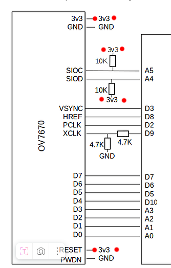
Всем привет! Новокек в арудино, собрать хочу камеру ova7670 sd. Вообщем проблема такая подключил камеру сд сохраняю фото, но нужно еще подключить rtc времени, а он ни в какую параллельно не хочет работать не могу сохранить файлы, и в принципе не понятно как это работает. КТо то может помочь дописать?
#include <avr/io.h>
#include <util/twi.h>
#include <util/delay.h>
#include <avr/pgmspace.h>

#include <Wire.h>
#include <SD.h>
#define SD_PIN 4

// pin 10
#define VSYNC 10
// pin 9
#define XCLK 9

static int count = 1;

// #define F_CPU 16000000UL
#define vga 0
#define qvga 1
#define qqvga 2
#define yuv422 0
#define rgb565 1
#define bayerRGB 2
#define camAddr_WR 0x42
#define camAddr_RD 0x43
/* Registers */
#define REG_GAIN 0x00                 /* Gain lower 8 bits (rest in vref) */
#define REG_BLUE 0x01                 /* blue gain */
#define REG_RED 0x02                  /* red gain */
#define REG_VREF 0x03                 /* Pieces of GAIN, VSTART, VSTOP */
#define REG_COM1 0x04                 /* Control 1 */
#define COM1_CCIR656 0x40             /* CCIR656 enable */
#define REG_BAVE 0x05                 /* U/B Average level */
#define REG_GbAVE 0x06                /* Y/Gb Average level */
#define REG_AECHH 0x07                /* AEC MS 5 bits */
#define REG_RAVE 0x08                 /* V/R Average level */
#define REG_COM2 0x09                 /* Control 2 */
#define COM2_SSLEEP 0x10              /* Soft sleep mode */
#define REG_PID 0x0a                  /* Product ID MSB */
#define REG_VER 0x0b                  /* Product ID LSB */
#define REG_COM3 0x0c                 /* Control 3 */
#define COM3_SWAP 0x40                /* Byte swap */
#define COM3_SCALEEN 0x08             /* Enable scaling */
#define COM3_DCWEN 0x04               /* Enable downsamp/crop/window */
#define REG_COM4 0x0d                 /* Control 4 */
#define REG_COM5 0x0e                 /* All "reserved" */
#define REG_COM6 0x0f                 /* Control 6 */
#define REG_AECH 0x10                 /* More bits of AEC value */
#define REG_CLKRC 0x11                /* Clocl control */
#define CLK_EXT 0x40                  /* Use external clock directly */
#define CLK_SCALE 0x3f                /* Mask for internal clock scale */
#define REG_COM7 0x12 /* Control 7 */ // REG mean address.
#define COM7_RESET 0x80               /* Register reset */
#define COM7_FMT_MASK 0x38
#define COM7_FMT_VGA 0x00
#define COM7_FMT_CIF 0x20   /* CIF format */
#define COM7_FMT_QVGA 0x10  /* QVGA format */
#define COM7_FMT_QCIF 0x08  /* QCIF format */
#define COM7_RGB 0x04       /* bits 0 and 2 - RGB format */
#define COM7_YUV 0x00       /* YUV */
#define COM7_BAYER 0x01     /* Bayer format */
#define COM7_PBAYER 0x05    /* "Processed bayer" */
#define REG_COM8 0x13       /* Control 8 */
#define COM8_FASTAEC 0x80   /* Enable fast AGC/AEC */
#define COM8_AECSTEP 0x40   /* Unlimited AEC step size */
#define COM8_BFILT 0x20     /* Band filter enable */
#define COM8_AGC 0x04       /* Auto gain enable */
#define COM8_AWB 0x02       /* White balance enable */
#define COM8_AEC 0x01       /* Auto exposure enable */
#define REG_COM9 0x14       /* Control 9- gain ceiling */
#define REG_COM10 0x15      /* Control 10 */
#define COM10_HSYNC 0x40    /* HSYNC instead of HREF */
#define COM10_PCLK_HB 0x20  /* Suppress PCLK on horiz blank */
#define COM10_HREF_REV 0x08 /* Reverse HREF */
#define COM10_VS_LEAD 0x04  /* VSYNC on clock leading edge */
#define COM10_VS_NEG 0x02   /* VSYNC negative */
#define COM10_HS_NEG 0x01   /* HSYNC negative */
#define REG_HSTART 0x17     /* Horiz start high bits */
#define REG_HSTOP 0x18      /* Horiz stop high bits */
#define REG_VSTART 0x19     /* Vert start high bits */
#define REG_VSTOP 0x1a      /* Vert stop high bits */
#define REG_PSHFT 0x1b      /* Pixel delay after HREF */
#define REG_MIDH 0x1c       /* Manuf. ID high */
#define REG_MIDL 0x1d       /* Manuf. ID low */
#define REG_MVFP 0x1e       /* Mirror / vflip */
#define MVFP_MIRROR 0x20    /* Mirror image */
#define MVFP_FLIP 0x10      /* Vertical flip */
#define REG_AEW 0x24        /* AGC upper limit */
#define REG_AEB 0x25        /* AGC lower limit */
#define REG_VPT 0x26        /* AGC/AEC fast mode op region */
#define REG_HSYST 0x30      /* HSYNC rising edge delay */
#define REG_HSYEN 0x31      /* HSYNC falling edge delay */
#define REG_HREF 0x32       /* HREF pieces */
#define REG_TSLB 0x3a       /* lots of stuff */
#define TSLB_YLAST 0x04     /* UYVY or VYUY - see com13 */
#define REG_COM11 0x3b      /* Control 11 */
#define COM11_NIGHT 0x80    /* NIght mode enable */
#define COM11_NMFR 0x60     /* Two bit NM frame rate */
#define COM11_HZAUTO 0x10   /* Auto detect 50/60 Hz */
#define COM11_50HZ 0x08     /* Manual 50Hz select */
#define COM11_EXP 0x02
#define REG_COM12 0x3c     /* Control 12 */
#define COM12_HREF 0x80    /* HREF always */
#define REG_COM13 0x3d     /* Control 13 */
#define COM13_GAMMA 0x80   /* Gamma enable */
#define COM13_UVSAT 0x40   /* UV saturation auto adjustment */
#define COM13_UVSWAP 0x01  /* V before U - w/TSLB */
#define REG_COM14 0x3e     /* Control 14 */
#define COM14_DCWEN 0x10   /* DCW/PCLK-scale enable */
#define REG_EDGE 0x3f      /* Edge enhancement factor */
#define REG_COM15 0x40     /* Control 15 */
#define COM15_R10F0 0x00   /* Data range 10 to F0 */
#define COM15_R01FE 0x80   /*      01 to FE */
#define COM15_R00FF 0xc0   /*      00 to FF */
#define COM15_RGB565 0x10  /* RGB565 output */
#define COM15_RGB555 0x30  /* RGB555 output */
#define REG_COM16 0x41     /* Control 16 */
#define COM16_AWBGAIN 0x08 /* AWB gain enable */
#define REG_COM17 0x42     /* Control 17 */
#define COM17_AECWIN 0xc0  /* AEC window - must match COM4 */
#define COM17_CBAR 0x08    /* DSP Color bar */
/*
 * This matrix defines how the colors are generated, must be
 * tweaked to adjust hue and saturation.
 *
 * Order: v-red, v-green, v-blue, u-red, u-green, u-blue
 * They are nine-bit signed quantities, with the sign bit
 * stored in0x58.Sign for v-red is bit 0, and up from there.
 */
#define REG_CMATRIX_BASE 0x4f
#define CMATRIX_LEN 6
#define REG_CMATRIX_SIGN 0x58
#define REG_BRIGHT 0x55   /* Brightness */
#define REG_CONTRAS 0x56  /* Contrast control */
#define REG_GFIX 0x69     /* Fix gain control */
#define REG_REG76 0x76    /* OV's name */
#define R76_BLKPCOR 0x80  /* Black pixel correction enable */
#define R76_WHTPCOR 0x40  /* White pixel correction enable */
#define REG_RGB444 0x8c   /* RGB 444 control */
#define R444_ENABLE 0x02  /* Turn on RGB444, overrides 5x5 */
#define R444_RGBX 0x01    /* Empty nibble at end */
#define REG_HAECC1 0x9f   /* Hist AEC/AGC control 1 */
#define REG_HAECC2 0xa0   /* Hist AEC/AGC control 2 */
#define REG_BD50MAX 0xa5  /* 50hz banding step limit */
#define REG_HAECC3 0xa6   /* Hist AEC/AGC control 3 */
#define REG_HAECC4 0xa7   /* Hist AEC/AGC control 4 */
#define REG_HAECC5 0xa8   /* Hist AEC/AGC control 5 */
#define REG_HAECC6 0xa9   /* Hist AEC/AGC control 6 */
#define REG_HAECC7 0xaa   /* Hist AEC/AGC control 7 */
#define REG_BD60MAX 0xab  /* 60hz banding step limit */
#define REG_GAIN 0x00     /* Gain lower 8 bits (rest in vref) */
#define REG_BLUE 0x01     /* blue gain */
#define REG_RED 0x02      /* red gain */
#define REG_VREF 0x03     /* Pieces of GAIN, VSTART, VSTOP */
#define REG_COM1 0x04     /* Control 1 */
#define COM1_CCIR656 0x40 /* CCIR656 enable */
#define REG_BAVE 0x05     /* U/B Average level */
#define REG_GbAVE 0x06    /* Y/Gb Average level */
#define REG_AECHH 0x07    /* AEC MS 5 bits */
#define REG_RAVE 0x08     /* V/R Average level */
#define REG_COM2 0x09     /* Control 2 */
#define COM2_SSLEEP 0x10  /* Soft sleep mode */
#define REG_PID 0x0a      /* Product ID MSB */
#define REG_VER 0x0b      /* Product ID LSB */
#define REG_COM3 0x0c     /* Control 3 */
#define COM3_SWAP 0x40    /* Byte swap */
#define COM3_SCALEEN 0x08 /* Enable scaling */
#define COM3_DCWEN 0x04   /* Enable downsamp/crop/window */
#define REG_COM4 0x0d     /* Control 4 */
#define REG_COM5 0x0e     /* All "reserved" */
#define REG_COM6 0x0f     /* Control 6 */
#define REG_AECH 0x10     /* More bits of AEC value */
#define REG_CLKRC 0x11    /* Clocl control */
#define CLK_EXT 0x40      /* Use external clock directly */
#define CLK_SCALE 0x3f    /* Mask for internal clock scale */
#define REG_COM7 0x12     /* Control 7 */
#define COM7_RESET 0x80   /* Register reset */
#define COM7_FMT_MASK 0x38
#define COM7_FMT_VGA 0x00
#define COM7_FMT_CIF 0x20   /* CIF format */
#define COM7_FMT_QVGA 0x10  /* QVGA format */
#define COM7_FMT_QCIF 0x08  /* QCIF format */
#define COM7_RGB 0x04       /* bits 0 and 2 - RGB format */
#define COM7_YUV 0x00       /* YUV */
#define COM7_BAYER 0x01     /* Bayer format */
#define COM7_PBAYER 0x05    /* "Processed bayer" */
#define REG_COM8 0x13       /* Control 8 */
#define COM8_FASTAEC 0x80   /* Enable fast AGC/AEC */
#define COM8_AECSTEP 0x40   /* Unlimited AEC step size */
#define COM8_BFILT 0x20     /* Band filter enable */
#define COM8_AGC 0x04       /* Auto gain enable */
#define COM8_AWB 0x02       /* White balance enable */
#define COM8_AEC 0x01       /* Auto exposure enable */
#define REG_COM9 0x14       /* Control 9- gain ceiling */
#define REG_COM10 0x15      /* Control 10 */
#define COM10_HSYNC 0x40    /* HSYNC instead of HREF */
#define COM10_PCLK_HB 0x20  /* Suppress PCLK on horiz blank */
#define COM10_HREF_REV 0x08 /* Reverse HREF */
#define COM10_VS_LEAD 0x04  /* VSYNC on clock leading edge */
#define COM10_VS_NEG 0x02   /* VSYNC negative */
#define COM10_HS_NEG 0x01   /* HSYNC negative */
#define REG_HSTART 0x17     /* Horiz start high bits */
#define REG_HSTOP 0x18      /* Horiz stop high bits */
#define REG_VSTART 0x19     /* Vert start high bits */
#define REG_VSTOP 0x1a      /* Vert stop high bits */
#define REG_PSHFT 0x1b      /* Pixel delay after HREF */
#define REG_MIDH 0x1c       /* Manuf. ID high */
#define REG_MIDL 0x1d       /* Manuf. ID low */
#define REG_MVFP 0x1e       /* Mirror / vflip */
#define MVFP_MIRROR 0x20    /* Mirror image */
#define MVFP_FLIP 0x10      /* Vertical flip */
#define REG_AEW 0x24        /* AGC upper limit */
#define REG_AEB 0x25        /* AGC lower limit */
#define REG_VPT 0x26        /* AGC/AEC fast mode op region */
#define REG_HSYST 0x30      /* HSYNC rising edge delay */
#define REG_HSYEN 0x31      /* HSYNC falling edge delay */
#define REG_HREF 0x32       /* HREF pieces */
#define REG_TSLB 0x3a       /* lots of stuff */
#define TSLB_YLAST 0x04     /* UYVY or VYUY - see com13 */
#define REG_COM11 0x3b      /* Control 11 */
#define COM11_NIGHT 0x80    /* NIght mode enable */
#define COM11_NMFR 0x60     /* Two bit NM frame rate */
#define COM11_HZAUTO 0x10   /* Auto detect 50/60 Hz */
#define COM11_50HZ 0x08     /* Manual 50Hz select */
#define COM11_EXP 0x02
#define REG_COM12 0x3c     /* Control 12 */
#define COM12_HREF 0x80    /* HREF always */
#define REG_COM13 0x3d     /* Control 13 */
#define COM13_GAMMA 0x80   /* Gamma enable */
#define COM13_UVSAT 0x40   /* UV saturation auto adjustment */
#define COM13_UVSWAP 0x01  /* V before U - w/TSLB */
#define REG_COM14 0x3e     /* Control 14 */
#define COM14_DCWEN 0x10   /* DCW/PCLK-scale enable */
#define REG_EDGE 0x3f      /* Edge enhancement factor */
#define REG_COM15 0x40     /* Control 15 */
#define COM15_R10F0 0x00   /* Data range 10 to F0 */
#define COM15_R01FE 0x80   /*      01 to FE */
#define COM15_R00FF 0xc0   /*      00 to FF */
#define COM15_RGB565 0x10  /* RGB565 output */
#define COM15_RGB555 0x30  /* RGB555 output */
#define REG_COM16 0x41     /* Control 16 */
#define COM16_AWBGAIN 0x08 /* AWB gain enable */
#define REG_COM17 0x42     /* Control 17 */
#define COM17_AECWIN 0xc0  /* AEC window - must match COM4 */
#define COM17_CBAR 0x08    /* DSP Color bar */
#define CMATRIX_LEN 6
#define REG_BRIGHT 0x55  /* Brightness */
#define REG_REG76 0x76   /* OV's name */
#define R76_BLKPCOR 0x80 /* Black pixel correction enable */
#define R76_WHTPCOR 0x40 /* White pixel correction enable */
#define REG_RGB444 0x8c  /* RGB 444 control */
#define R444_ENABLE 0x02 /* Turn on RGB444, overrides 5x5 */
#define R444_RGBX 0x01   /* Empty nibble at end */
#define REG_HAECC1 0x9f  /* Hist AEC/AGC control 1 */
#define REG_HAECC2 0xa0  /* Hist AEC/AGC control 2 */
#define REG_BD50MAX 0xa5 /* 50hz banding step limit */
#define REG_HAECC3 0xa6  /* Hist AEC/AGC control 3 */
#define REG_HAECC4 0xa7  /* Hist AEC/AGC control 4 */
#define REG_HAECC5 0xa8  /* Hist AEC/AGC control 5 */
#define REG_HAECC6 0xa9  /* Hist AEC/AGC control 6 */
#define REG_HAECC7 0xaa  /* Hist AEC/AGC control 7 */
#define REG_BD60MAX 0xab /* 60hz banding step limit */
#define MTX1 0x4f        /* Matrix Coefficient 1 */
#define MTX2 0x50        /* Matrix Coefficient 2 */
#define MTX3 0x51        /* Matrix Coefficient 3 */
#define MTX4 0x52        /* Matrix Coefficient 4 */
#define MTX5 0x53        /* Matrix Coefficient 5 */
#define MTX6 0x54        /* Matrix Coefficient 6 */
#define REG_CONTRAS 0x56 /* Contrast control */
#define MTXS 0x58        /* Matrix Coefficient Sign */
#define AWBC7 0x59       /* AWB Control 7 */
#define AWBC8 0x5a       /* AWB Control 8 */
#define AWBC9 0x5b       /* AWB Control 9 */
#define AWBC10 0x5c      /* AWB Control 10 */
#define AWBC11 0x5d      /* AWB Control 11 */
#define AWBC12 0x5e      /* AWB Control 12 */
#define REG_GFI 0x69     /* Fix gain control */
#define GGAIN 0x6a       /* G Channel AWB Gain */
#define DBLV 0x6b
#define AWBCTR3 0x6c /* AWB Control 3 */
#define AWBCTR2 0x6d /* AWB Control 2 */
#define AWBCTR1 0x6e /* AWB Control 1 */
#define AWBCTR0 0x6f /* AWB Control 0 */
struct regval_list
{
    uint8_t reg_num;
    uint16_t value;
};
const struct regval_list qvga_ov7670[] PROGMEM = {
    {REG_COM14, 0x19},
    {0x72, 0x11},
    {0x73, 0xf1},
    {REG_HSTART, 0x16},
    {REG_HSTOP, 0x04},
    {REG_HREF, 0xa4},
    {REG_VSTART, 0x02},
    {REG_VSTOP, 0x7a},
    {REG_VREF, 0x0a},
    {0xff, 0xff}, /* END MARKER */
};
const struct regval_list yuv422_ov7670[] PROGMEM = {
    {REG_COM7, 0x0}, /* Selects YUV mode */
    {REG_RGB444, 0}, /* No RGB444 please */
    {REG_COM1, 0},
    {REG_COM15, COM15_R00FF},
    {REG_COM9, 0x6A}, /* 128x gain ceiling; 0x8 is reserved bit */
    {0x4f, 0x80},     /* "matrix coefficient 1" */
    {0x50, 0x80},     /* "matrix coefficient 2" */
    {0x51, 0},        /* vb */
    {0x52, 0x22},     /* "matrix coefficient 4" */
    {0x53, 0x5e},     /* "matrix coefficient 5" */
    {0x54, 0x80},     /* "matrix coefficient 6" */
    {REG_COM13, COM13_UVSAT},
    {0xff, 0xff}, /* END MARKER */
};
const struct regval_list ov7670_default_regs[] PROGMEM = {
    // from the linux driver
    {REG_COM7, COM7_RESET},
    {REG_TSLB, 0x04}, /* OV */
    {REG_COM7, 0},    /* VGA */
    /*
     * Set the hardware window.  These values from OV don't entirely
     * make sense - hstop is less than hstart.  But they work...
     */
    {REG_HSTART, 0x13},
    {REG_HSTOP, 0x01},
    {REG_HREF, 0xb6},
    {REG_VSTART, 0x02},
    {REG_VSTOP, 0x7a},
    {REG_VREF, 0x0a},
    {REG_COM3, 0},
    {REG_COM14, 0},
    /* Mystery scaling numbers */
    {0x70, 0x3a},
    {0x71, 0x35},
    {0x72, 0x11},
    {0x73, 0xf0},
    {0xa2, /* 0x02 changed to 1*/ 1},
    {REG_COM10, 0x0},
    /* Gamma curve values */
    {0x7a, 0x20},
    {0x7b, 0x10},
    {0x7c, 0x1e},
    {0x7d, 0x35},
    {0x7e, 0x5a},
    {0x7f, 0x69},
    {0x80, 0x76},
    {0x81, 0x80},
    {0x82, 0x88},
    {0x83, 0x8f},
    {0x84, 0x96},
    {0x85, 0xa3},
    {0x86, 0xaf},
    {0x87, 0xc4},
    {0x88, 0xd7},
    {0x89, 0xe8},
    /* AGC and AEC parameters.  Note we start by disabling those features,
    then turn them only after tweaking the values. */
    {REG_COM8, COM8_FASTAEC | COM8_AECSTEP},
    {REG_GAIN, 0},
    {REG_AECH, 0},
    {REG_COM4, 0x40}, /* magic reserved bit */
    {REG_COM9, 0x18}, /* 4x gain + magic rsvd bit */
    {REG_BD50MAX, 0x05},
    {REG_BD60MAX, 0x07},
    {REG_AEW, 0x95},
    {REG_AEB, 0x33},
    {REG_VPT, 0xe3},
    {REG_HAECC1, 0x78},
    {REG_HAECC2, 0x68},
    {0xa1, 0x03}, /* magic */
    {REG_HAECC3, 0xd8},
    {REG_HAECC4, 0xd8},
    {REG_HAECC5, 0xf0},
    {REG_HAECC6, 0x90},
    {REG_HAECC7, 0x94},
    {REG_COM8, COM8_FASTAEC | COM8_AECSTEP | COM8_AGC | COM8_AEC},
    {0x30, 0},
    {0x31, 0}, // disable some delays
    /* Almost all of these are magic "reserved" values.  */
    {REG_COM5, 0x61},
    {REG_COM6, 0x4b},
    {0x16, 0x02},
    {REG_MVFP, 0x07},
    {0x21, 0x02},
    {0x22, 0x91},
    {0x29, 0x07},
    {0x33, 0x0b},
    {0x35, 0x0b},
    {0x37, 0x1d},
    {0x38, 0x71},
    {0x39, 0x2a},
    {REG_COM12, 0x78},
    {0x4d, 0x40},
    {0x4e, 0x20},
    {REG_GFIX, 0},
    /*{0x6b, 0x4a},*/ {0x74, 0x10},
    {0x8d, 0x4f},
    {0x8e, 0},
    {0x8f, 0},
    {0x90, 0},
    {0x91, 0},
    {0x96, 0},
    {0x9a, 0},
    {0xb0, 0x84},
    {0xb1, 0x0c},
    {0xb2, 0x0e},
    {0xb3, 0x82},
    {0xb8, 0x0a},
    /* More reserved magic, some of which tweaks white balance */
    {0x43, 0x0a},
    {0x44, 0xf0},
    {0x45, 0x34},
    {0x46, 0x58},
    {0x47, 0x28},
    {0x48, 0x3a},
    {0x59, 0x88},
    {0x5a, 0x88},
    {0x5b, 0x44},
    {0x5c, 0x67},
    {0x5d, 0x49},
    {0x5e, 0x0e},
    {0x6c, 0x0a},
    {0x6d, 0x55},
    {0x6e, 0x11},
    {0x6f, 0x9e}, /* it was 0x9F "9e for advance AWB" */
    {0x6a, 0x40},
    {REG_BLUE, 0x40},
    {REG_RED, 0x60},
    {REG_COM8, COM8_FASTAEC | COM8_AECSTEP | COM8_AGC | COM8_AEC | COM8_AWB},
    /* Matrix coefficients */
    {0x4f, 0x80},
    {0x50, 0x80},
    {0x51, 0},
    {0x52, 0x22},
    {0x53, 0x5e},
    {0x54, 0x80},
    {0x58, 0x9e},
    {REG_COM16, COM16_AWBGAIN},
    {REG_EDGE, 0},
    {0x75, 0x05},
    {REG_REG76, 0xe1},
    {0x4c, 0},
    {0x77, 0x01},
    {REG_COM13, /*0xc3*/ 0x48},
    {0x4b, 0x09},
    {0xc9, 0x60}, /*{REG_COM16, 0x38},*/
    {0x56, 0x40},
    {0x34, 0x11},
    {REG_COM11, COM11_EXP | COM11_HZAUTO},
    {0xa4, 0x82 /*Was 0x88*/},
    {0x96, 0},
    {0x97, 0x30},
    {0x98, 0x20},
    {0x99, 0x30},
    {0x9a, 0x84},
    {0x9b, 0x29},
    {0x9c, 0x03},
    {0x9d, 0x4c},
    {0x9e, 0x3f},
    {0x78, 0x04},
    /* Extra-weird stuff.  Some sort of multiplexor register */
    {0x79, 0x01},
    {0xc8, 0xf0},
    {0x79, 0x0f},
    {0xc8, 0x00},
    {0x79, 0x10},
    {0xc8, 0x7e},
    {0x79, 0x0a},
    {0xc8, 0x80},
    {0x79, 0x0b},
    {0xc8, 0x01},
    {0x79, 0x0c},
    {0xc8, 0x0f},
    {0x79, 0x0d},
    {0xc8, 0x20},
    {0x79, 0x09},
    {0xc8, 0x80},
    {0x79, 0x02},
    {0xc8, 0xc0},
    {0x79, 0x03},
    {0xc8, 0x40},
    {0x79, 0x05},
    {0xc8, 0x30},
    {0x79, 0x26},
    {0xff, 0xff}, /* END MARKER */
};
void error_led(void)
{
    DDRB |= 32; // make sure led is output
    while (1)
    {                // wait for reset
        PORTB ^= 32; // toggle led
        _delay_ms(100);
    }
}
void twiStart(void)
{
    TWCR = _BV(TWINT) | _BV(TWSTA) | _BV(TWEN); // send start
    while (!(TWCR & (1 << TWINT)))
        ; // wait for start to be transmitted
    if ((TWSR & 0xF8) != TW_START)
        error_led();
}
void twiWriteByte(uint8_t DATA, uint8_t type)
{
    TWDR = DATA;
    TWCR = _BV(TWINT) | _BV(TWEN);
    while (!(TWCR & (1 << TWINT)))
    {
    }
    if ((TWSR & 0xF8) != type)
        error_led();
}
void twiAddr(uint8_t addr, uint8_t typeTWI)
{
    TWDR = addr;                   // send address
    TWCR = _BV(TWINT) | _BV(TWEN); /* clear interrupt to start transmission */
    while ((TWCR & _BV(TWINT)) == 0)
        ; /* wait for transmission */
    if ((TWSR & 0xF8) != typeTWI)
        error_led();
}
void writeReg(uint8_t reg, uint8_t dat)
{
    // send start condition
    twiStart();
    twiAddr(camAddr_WR, TW_MT_SLA_ACK);
    twiWriteByte(reg, TW_MT_DATA_ACK);
    twiWriteByte(dat, TW_MT_DATA_ACK);
    TWCR = (1 << TWINT) | (1 << TWEN) | (1 << TWSTO); // send stop
    _delay_ms(1);
}
static uint8_t twiRd(uint8_t nack)
{
    if (nack)
    {
        TWCR = _BV(TWINT) | _BV(TWEN);
        while ((TWCR & _BV(TWINT)) == 0)
            ; /* wait for transmission */
        if ((TWSR & 0xF8) != TW_MR_DATA_NACK)
            error_led();
        return TWDR;
    }
    else
    {
        TWCR = _BV(TWINT) | _BV(TWEN) | _BV(TWEA);
        while ((TWCR & _BV(TWINT)) == 0)
            ; /* wait for transmission */
        if ((TWSR & 0xF8) != TW_MR_DATA_ACK)
            error_led();
        return TWDR;
    }
}
uint8_t rdReg(uint8_t reg)
{
    uint8_t dat;
    twiStart();
    twiAddr(camAddr_WR, TW_MT_SLA_ACK);
    twiWriteByte(reg, TW_MT_DATA_ACK);
    TWCR = (1 << TWINT) | (1 << TWEN) | (1 << TWSTO); // send stop
    _delay_ms(1);
    twiStart();
    twiAddr(camAddr_RD, TW_MR_SLA_ACK);
    dat = twiRd(1);
    TWCR = (1 << TWINT) | (1 << TWEN) | (1 << TWSTO); // send stop
    _delay_ms(1);
    return dat;
}
void wrSensorRegs8_8(const struct regval_list reglist[])
{
    uint8_t reg_addr, reg_val;
    const struct regval_list *next = reglist;
    while ((reg_addr != 0xff) | (reg_val != 0xff))
    {
        reg_addr = pgm_read_byte(&next->reg_num);
        reg_val = pgm_read_byte(&next->value);
        writeReg(reg_addr, reg_val);
        next++;
    }
}
void setColor(void)
{
    wrSensorRegs8_8(yuv422_ov7670);
    // wrSensorRegs8_8(qvga_ov7670);
}
void setResolution(void)
{
    writeReg(REG_COM3, 4); // REG_COM3 enable scaling
    wrSensorRegs8_8(qvga_ov7670);
}
void camInit(void)
{
    writeReg(0x12, 0x80);
    _delay_ms(100);
    wrSensorRegs8_8(ov7670_default_regs);
    writeReg(REG_COM10, 32); // PCLK does not toggle on HBLANK.
}
void arduinoUnoInut(void)
{
    cli(); // disable interrupts
    /* Setup the 8mhz PWM clock
     * This will be on pin 11*/
    // // DDRB |= (1 << 3); // pin 11
    DDRB |= (1 << 1); // pin 9
    ASSR &= ~(_BV(EXCLK) | _BV(AS2));
    // // TCCR2A = (1 << COM2A0) | (1 << WGM21) | (1 << WGM20);  // pin 11
    // // TCCR2B = (1 << WGM22) | (1 << CS20);  // pin 11
    // // OCR2A = 0;   //(F_CPU)/(2*(X+1))  // pin 11
    TCCR1A = (1 << COM1A0) | (1 << WGM11) | (1 << WGM10); // pin 9
    TCCR1B = (1 << WGM13) | (1 << WGM12) | (1 << CS10);   // pin 9
    OCR1A = 0;                                            // pin 9
    /////
    DDRC &= ~15; // low d0-d3 camera

    // old pin4
    //// DDRD &= ~252; // d7-d4 and interrupt pins
    // pin 10
    DDRB &= ~(1 << DDB2);
    _delay_ms(3000);
    // set up twi for 100khz
    TWSR &= ~3; // disable prescaler for TWI
    TWBR = 72;  // set to 100khz
    // enable serial
    UBRR0H = 0;
    UBRR0L = 1;                           // 0 = 2M baud rate. 1 = 1M baud. 3 = 0.5M. 7 = 250k 207 is 9600 baud rate.
    UCSR0A |= 2;                          // double speed aysnc
    UCSR0B = (1 << RXEN0) | (1 << TXEN0); // Enable receiver and transmitter
    UCSR0C = 6;                           // async 1 stop bit 8bit char no parity bits
}
static void captureImg(String title)
{
    delay(1000);
    Serial.print("\nStart screen " + title);
    int h, w;
    if (SD.exists(title))
    {
        SD.remove(title);
    }
    File dataFile = SD.open(title, FILE_WRITE);
    delay(100);
    while (!(PIND & 8))
        ; // wait for high
    while ((PIND & 8))
        ; // wait for low

    h = 240;
    while (h--)
    {
        w = 320;
        byte dataBuffer[320];
        while (w--)
        {
            while ((PIND & 4))
                ; // wait for low
            dataBuffer[319 - w] = (PINC & 15) | (PIND & 240);

            while (!(PIND & 4))
                ; // wait for high
            while ((PIND & 4))
                ; // wait for low
            while (!(PIND & 4))
                ; // wait for high
        }
        dataFile.write(dataBuffer, 320);
    }

    dataFile.flush();
    dataFile.close();
    delay(100);
    Serial.print("\nFinish screen " + title);
}

void setup()
{
    arduinoUnoInut();
    camInit();
    setResolution();
    setColor();
    writeReg(0x11, 0x1F); // Earlier it had the value:writeReg(0x11, 12); New version works better for me :) !!!!
    interrupts();
    Serial.begin(9600);
    delay(100);
    Serial.print("\nStart SD");
    while (!SD.begin(SD_PIN))
    {
        Serial.print(".");
        delay(500);
    }
    Serial.print("\nSD started");
    Serial.print("\nWaiting cam warm up");
    delay(15000);
}
void loop()
{
    captureImg(String(count) + ".raw");
    count++;
    if (count > 10) {
        Serial.print("\nFINISH");
        while(1);
    }
}```